Formulae
Key formulas go here.
Semiconductor Devices
PN Junction
When a p-type semiconductor is joined to an n-type semiconductor, a junction is formed called p-n junction. As soon as the p-n junction is formed, the electron from the N-region diffuse into the p-region where the combine withthe holes & gets neutralized. Similarly, the holes from the p-region diffuse into the N-region and combine with electrons to get neutralized. The P-region nearthe junction is left with immobile negative ions & N-region near the junction with immobile positive ions due to electron hole recombination. So, a thin layer around the junction becomes depleted of free charge carrier. This region where no free charge carriers are available is called a depletion region.
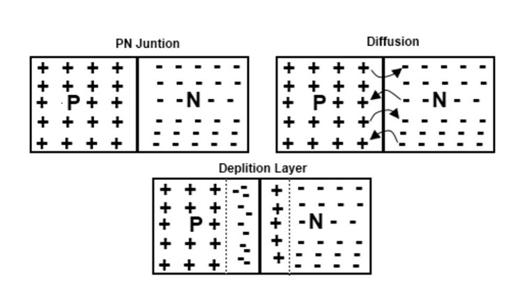
These collection of positive and negative charges at the junction sets up potential difference across the junction which is called Potential barrier. Thus, the potential difference developed across the junction due to diffusion of charges carriers is called potential barrier. It opposes further diffusion of free charge carriers into opposite region. Its value depends on the nature of the material, its temperature and doping concentration. Eg., the potential barrier across Ge is 0.3V and across Si is 0.7V.
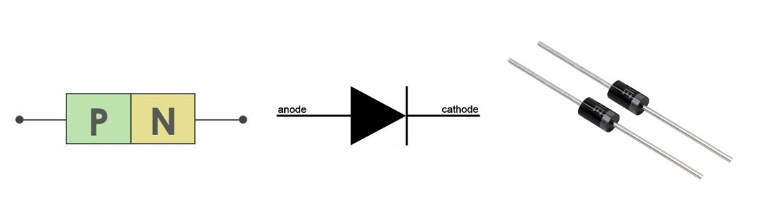
PN Junction Diode
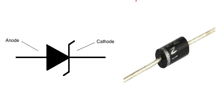
A device in which p-type semiconductor has a junction with a n-type semiconductor is called p-n junction diode. Its circuit symbol is shown below.The arrow gives the direction from p to the n-junction. The p-type region is anode and the n-type region is cathode.
Forward Biasing and Reverse Biasing
When an external potential difference is applied across p-n junction, the diode is said to be biased. There are two types of biasing.
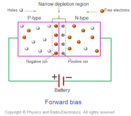
a. Forward Biasing: A p-n junction is said to be forward biased if the positive terminal of the external battery is connected to p-side and the negativeterminal to the n-side of the p-njunction. In forward biasing, theforward bias voltage opposes thepotential barrier. Thus, potential barrier is reduced & the depletionregion becomes thin. An electriccurrent flows across the diode due to migration of majority charge carrier called forward current. The diode offers very low resistance to the flow of current.
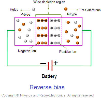
b. Reverse Biasing: A p-n junction diode is said to be reverse biased if the positive terminal of the external battery is connected to n-side and the negative terminal to the p-side of the p-n junction. In reverse biasing, the reverse bias voltage supports the potential barrier. Thus, potential barrier is increased & the depletion layer becomes thick. A small current flows across the diode due to migration of minority charge carrier called reverse current. The diode offers very high resistance to the flow of current.
Characteristics of p-n junction diode in Forward and Reverse Bias Condition
The graph between bias voltage across the PN junction diode & the current through it is called characteristics of the PN junction Diode. There are two types of characteristics of a PN junction diode.
a. Forward Bias Characteristics: The graph between forward bias voltageapplied to p-n jnction to the forward current through it is called forward bias characteristics.
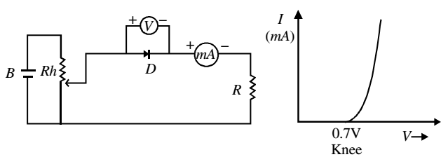
The forward characteristics can be studied byvarying the volatge across diode with the help ofrheostat & hence noting the corresponding forwardcurrent. The forward bias voltage is graduallyincreased and the corresponding forward current isnoted. It is found that as the forward bias voltage isincreased gradually, the current increases very slowlyuntil the potential barrier (0.3 V for Ge and 0.7V for Si)is overcome. If the forward bias voltage is furtherincreased, it overcomes the potential barrier & thecurrent increases rapidly. The forward bias voltage atwhich the current starts to increase rapidly is calledthe knee voltage (Vk).
a. Reverse Bias Characteristics: The graph between reverse biasvoltage applied to p-n junction to thereverse current through it is called reverse bias characteristics
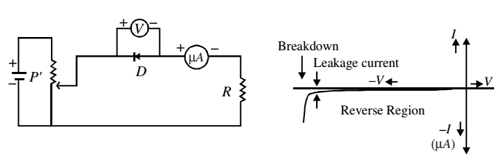
The reverse characteristics can bestudied by varying the voltage acrossdiode with the help of rheostat & hencenoting the corresponding reverse current.The reverse bias voltage is graduallyincreased & the corresponding reversecurrent is noted. It is found that as thereverse bias voltage is increased gradually,the current increases very slowly (almostconstant). At a particular high reverse biasvoltage, the current will increase abruptly.This reverse bias voltage is known asbreakdown voltage (VB).


Application of pn junction:
1. It is used as a rectifier.
2. It is used in voltage regulating circuit.
3. It is used as a switch in logic circuits.
Rectifier
Rectifier is a device used for converting alternating current into direct current. The process of converting ac into dc is called rectification. These are two types of rectifier: Half wave rectifier and Full wave rectifier
Half Wave Rectifier
The rectifier which convert only half cycle of ac into dc is called half wave rectifier. It works on the fact that the resistance of p-n junction becomes low when forward biased and becomes high when reversed biased.
The ac to be rectified is connected to the primary coil P1P2 of a transformer.S1S2 is the secondary coil of the same transformer where S1 is connected to p-side and S2 isconnected to n-side of the p-n junction. Output is taken across the load resistance RL.
During positive half cycle of input ac, let P1 is negative and P2 is positive. Due to induction, S1 becomes positive and S2 negative. Thus, p-n junction becomes forward biased & the resistance becomes low. Hence forward current flows & we get output.
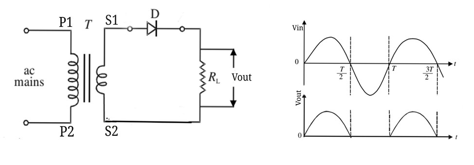
Similarly, during negative half cycle of inputac, P1 is positive and P2 is negative. Due to induction, S1 becomes negative and S2 becomes positive. Then, p-n junctionbecomes reverse biased & the resistance becomes high. Hence, there is no flow o fcurrent & thus we do not get output. In the output, we have current corresponding to half of the wave, the other half is missing. In this way, only unidirectional current flow through RL and it acts as the half wave rectifier.
Full Wave Rectifier
The rectifier which converts both positive & negative half cycle of ac into dc iscalled full wave rectifier. There are two types of full wave rectifier.: Centre Tapped Full wave rectifier and Bridge Rectifier
Centre Tapped Full Wave Rectifier
The arrangement for full wave rectifier using two p-n junction diode is shown below. The ac to be rectified is connected to the primary coil P1P2 of atransformer. S1S2 is the secondary coil of the same transformer where S1 is connected p-side of one diode & S2 is connected to p-side of another diode.The central tapping of the secondary coil is connected to n-side of both diodes through load resistance RL.
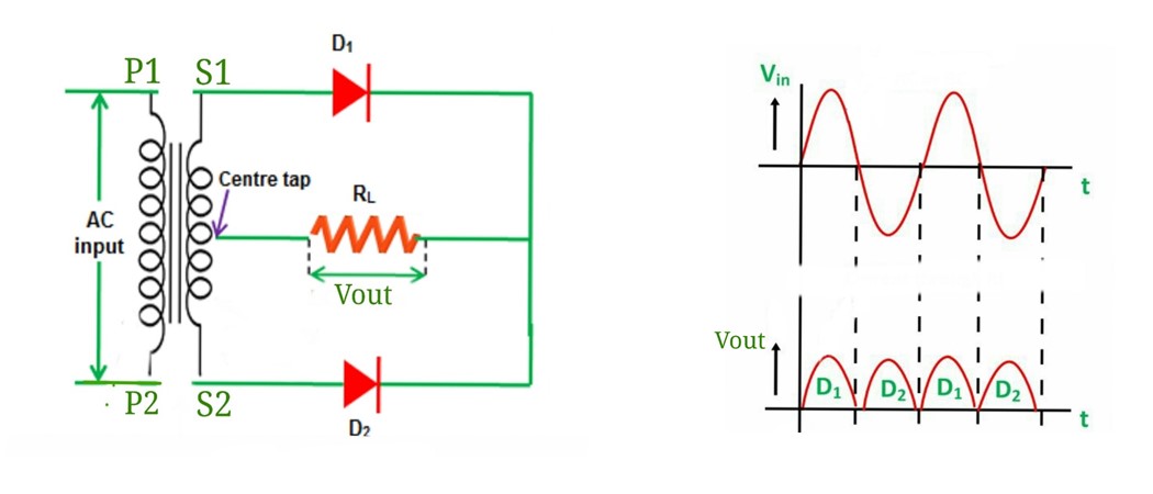
During positive half cycle of input ac, let P1 is negative and P2 is positive. Due to induction, S1 becomes positive & S2 becomes negative. Thus,upper diode becomes forward biased & lowerdiode becomes reverse biased. The forward current flows through upper diode in the given direction.
During negative half cycle of input ac, P1 is positive & P2 is negative. Due to induction, S1 becomes negative and S2 becomes positive. Thus,upper diode becomes reverse biased & lower diodebecomes forward biased. The forward currentflows through lower diode in the same direction asabove. Hence, in both half cycles, unidirectional current flows through RL.
Bridge Rectifier
The arrangement for full rectifer using for p-n junction diode is shown below. The ac to be rectified is connected to the primary coil P1P2 of atransformer. S1S2 is the secondary coil of the same transformer wherethe four diode are arranged in the form of bridge.
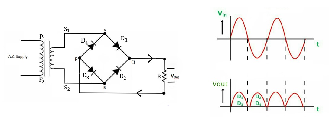
During positive half cycle of input ac, let P1 is negative & P2 is positive.Due to induction, S1 becomes positive & S2 becomes negative. Thus,diode D1 & D3 becomes forward biased & diode D2 & D4 becomes reversed biased. The forward current flows through diode D1 & D3 inthe given direction
During the negative half cycle of input ac, P1 is positive and P2 is negative. Due to induction, S1 becomes negative & S2 becomes positive. Thus, diode D1 and D3 becomes reverse biased & diode D2 and D4 becomes forward biased. The forward current flows through diode D2 and D4 in the same direction. Hence, in both half-cylce, unidirectional current flows through RL.
Filter Circuit
A rectifier output current by a rectifier contains ac & dc components. So, it is called pulsating dc. The circuit which removes the ac components & allow only the dc components to reach the load is called filter circuit.
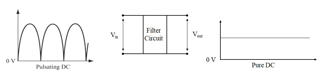
Some commonly used filter circuits are:
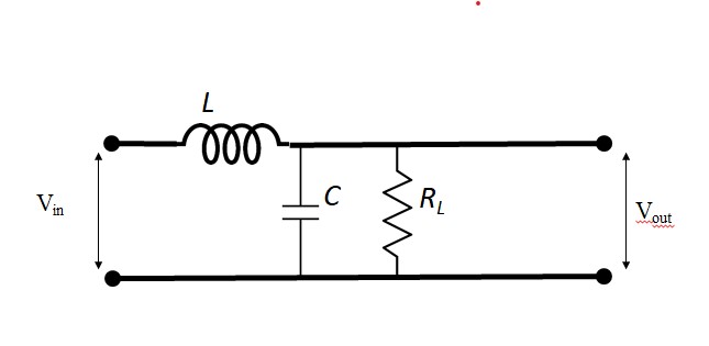
1. Inductor Filter: In this filter, an inductor is connected with load resistance RL. The input to the filter is the output from rectifier.
Since, inductive reactance, XL= 2πfL
For dc, f = 0
Thus, inductive reactance, XL = 0
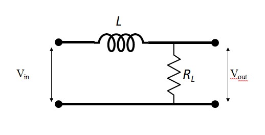
The inductor offer low resistance to dc & high resistance to ac. Hence, it allows dc component to pass & block the ac components. Therefore, we get only dccomponent across load resistance.
2. Capacitive Filter: In this filter, a capacitor is connected in parallel with load resistance RL. The input to the filter is the output from rectifier.
Since, capacitive reactance, XC= 1/2πfL
For dc, f = 0
Thus, capacitive reactance, XC = ∞
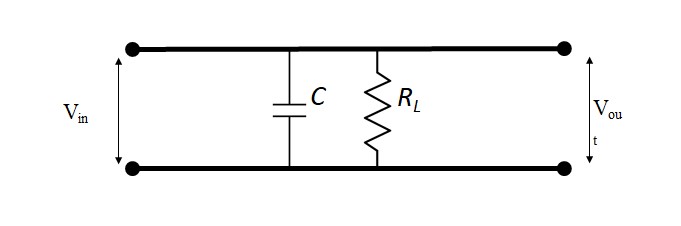
The capacitor offer high resistance to dc & low resistance to ac. Hence, it allows ac component to pass & block the dc components. Therefore, we get only dc component across load resistance.
3. LC Filter: In this filter, an inductor is connected in series with a parallel combination of capacitor & load resistor. The input to the filter is the output from rectifier.
The inductor blocks the ac component to pass & allow only dc to pass. The capacitor allows only ac to pass & block the dc component. Thus we get only dc component across load resistance.
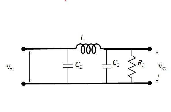
4. π Filter: It consists of two capacitors and an inductor connected in the form of π.The capacitor allows only ac component to pass through it & block the dc component. The inductor allows dc component to pass & blocks the ac component to pass through it. Thus, due to this combination, only dc component will remain across the load resistance.
Reverse Breakdown
There are two main processes by which reverse breakdown may occur: Avalanche Breakdown and Zener Breakdown
Avalanche Breakdown
The holes in the n-side & the conduction electrons in the p-side (minority charge) acquires sufficient kinetic energy from the reverse bias voltage collides with valence electrons & covalent bond will be broken. Thus, a hole-electron pair will be created. Breakdown occurring in this manner is called avalanche breakdown.
Zener Breakdown
In a heavily doped junction diode, the depletion region is thin. The reverse bias voltage breaks the covalent bond directly due to high electric field. Thus, a hole-electron pair will be created. Breakdown occurring in this manner is called zener breakdown.
Zener Diode
It is a specially designed heavily doped p-n junction diode which can operate continuously without being damaged in the region of reverse breakdown voltage.
In the reverse breakdown region, the voltage across the Zener diode remains constant even if the current through Zener diode increases. The circuit symbol of Zener diode is as
Characteristics of Zener Diode
The graph between bias voltage & the current through Zener diode is called characteristics of Zener diode.
The first quadrant is the forward biased region. Here the Zener diode acts like an ordinary diode. When a forward voltage is applied, current flows through it. But due to higher doping concentration, higher current flows through the Zener diode.
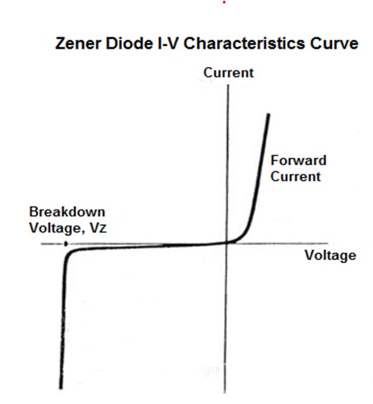
In the third quadrant, the Zener breakdown voltage is the reverse bias voltage after which a significant amount of current starts flowing through the Zener diode. Here in the diagram, VZ refers to the Zener breakdown voltage. Until the voltage reaches Zener breakdown level, tiny amount of current flows through the diode. This current is called leakage current. Once the reverse bias voltage becomes more than the Zener breakdown voltage, a significant amount of current starts flowing through the diode due to Zener breakdown. The voltage remains constant at the Zener breakdown voltage value, but the current through the diode increases when the input voltage gets increased. Due to this unique property of Zener diode, the depletion region regains its original position when the reverse voltage gets removed. The Zener diode doesn't get damaged despite this massive amount of current flowing through it. This unique functionality makes it very useful for many applications.
Zener Diode as a Voltage regulator
A Zener diode is sometimes called a voltage regulator diode because it maintain a constant output voltage even through the current through it changes. This is the principle behind the action of Zener diode as a voltage regulator.
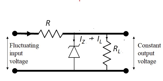
If the input voltage is increased, then I also increases. Thus, the additional increased current passes through Zener diode by increasing IZ keeping the current through load IL constant. Hence, the outpur voltage remains constant.
Similarly, when the load resistance RL increases, the load current IL decreases by increasing the current through Zener diode. IZ such that the output voltage remains constant. Since, voltage regulator is an electronic device which provides a constant voltage from a source. Hence, Zener diode acts as a voltage regulator.
Logic Gates
A digital circuit which either allows a signal to pass or stop through it when some logical conditions are satisfied are called logic gates.The basic logic gates are of three types:
OR Gate
It is a device that has two or more inputs & one output. The logic symbol & truth table for OR gate is given below:
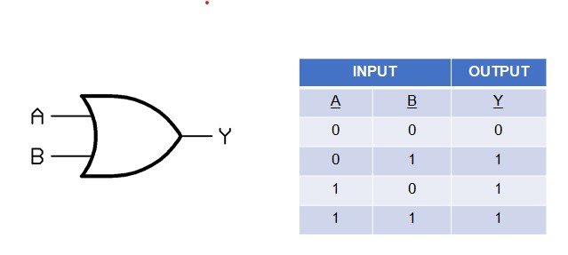
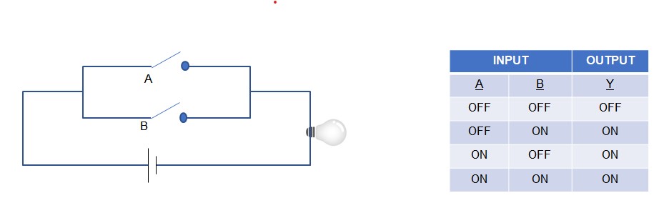
The OR gate is equivalent to two switch keys is parallel. Current flows only when A or B or both A & B are ON. No Current flows when A & B both are off.
Boolean expression for OR Gate is Y = A+B
AND Gate
It is a device that has two or more inputs & one output. The logic symbol & truth table for AND gate is given below:
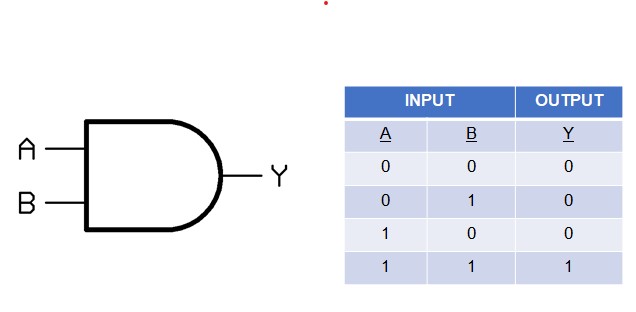
The AND gate is equivalent to two switch keys is series. Current flows only when both A & B are ON. No Current flows when any switch A or B or both is off.
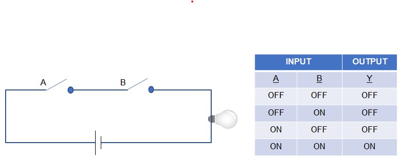
Boolean expression for AND Gate is Y = A.B
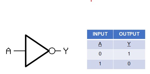
NOT Gate
It is a device that has only one input & one output. The logic symbol & truth table for NOT gate is given below:
The NOT gate is equivalent to the circuit shown below. The bulb will glow when switch A is OFF & it will not glow if it is ON.
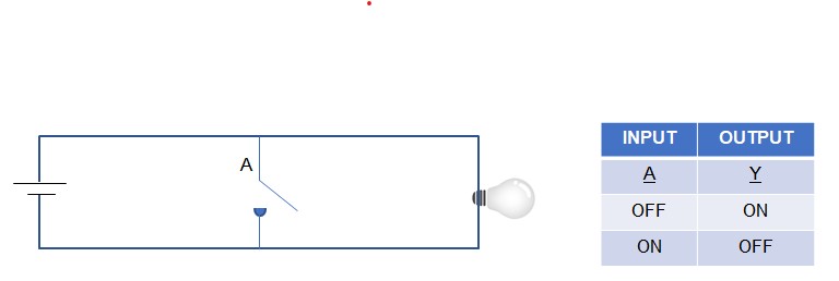
Boolean expression for NOT Gate is Y= Ā
Combination of GATES
Various combinations of three basic gates (OR, AND and NOT) provides us large no. of complicated digital circuits which are also known as gates. A few among them are:
NAND Gate
If we connect the output of AND gate to the input of a NOT gate, then the gate so obtained is called NAND gate. The logic symbol of truth table for NAND gate is given below:
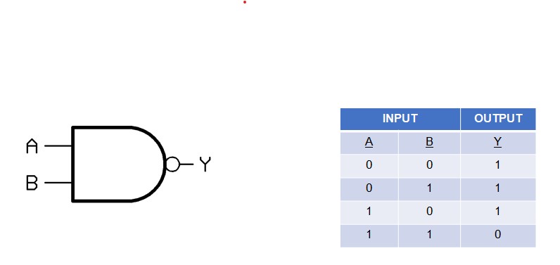
Boolean expression for NAND Gate is Y= (A.B)'
NOR Gate
If we connect the output of OR gate to the input of a NOT gate, then the gate so obtained is called NOR gate. The logic symbol of truth table for NOR gate is given below:
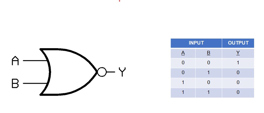
Boolean expression for NAND Gate is Y= (A+B)'
NAND Gate as Universal Gate
The NAND gate is a universal gate because its repeated use can give all other gates like OR, AND & NOT.
NOT gate from NAND Gate
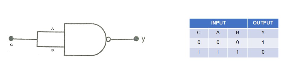
When two inputs of NAND gate are joined together so that it has one input, the resulting circuit is NOT gate.
AND gate from NAND Gate
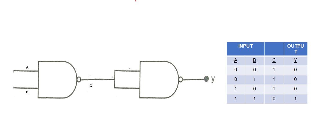
When output of 1st NAND gate is given to both input of 2nd NAND gate, then the resulting circuit is AND gate.
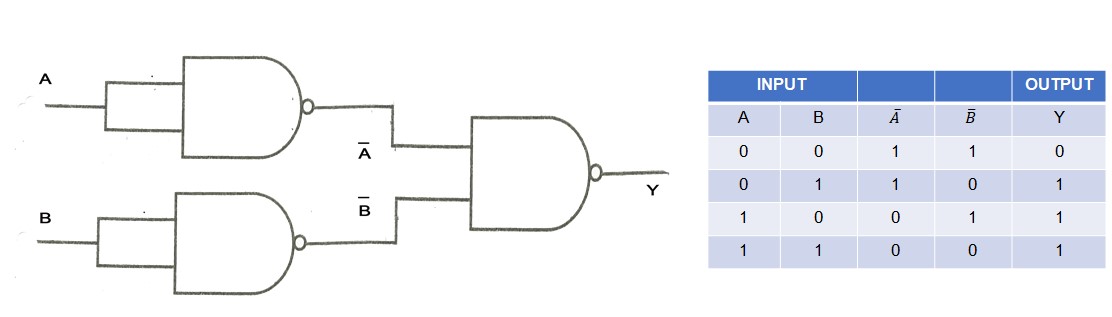
OR gate from NAND Gate
When two NAND gate are operated as NOT gate & their output is given to third NAND gate, then the resulting circuit is OR gate.